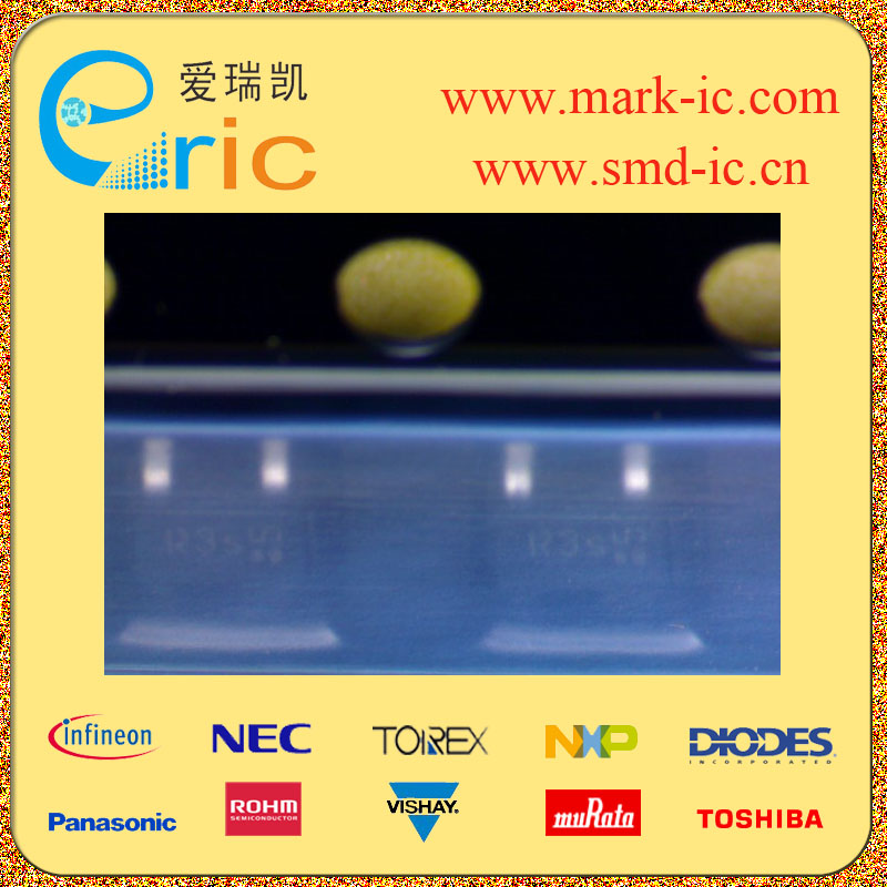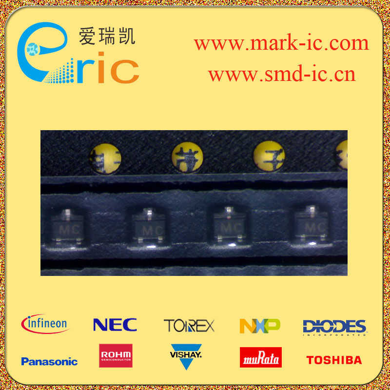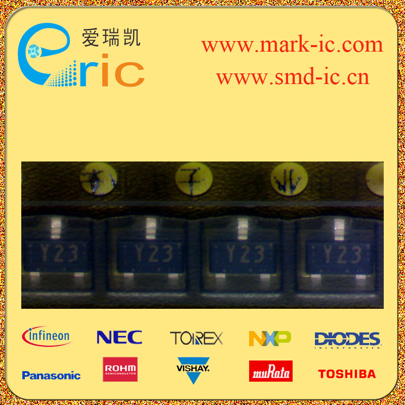
FDG6332C 复合场效应管 20V/-20V 700mA/-600mA SOT-363/SC70-6 marking/标记 32T DC/DC转换器 负载开关 逆变器
| 最大源漏极电压VdsDrain-Source Voltage | 20V/-20V |
| 最大栅源极电压Vgs(±)Gate-Source Voltage | 12V/12V |
| 最大漏极电流IdDrain Current | 700mA/-600mA |
| 源漏极导通电阻RdsDrain-Source On-State Resistance | 400mΩ@ VGS =2.5V, ID =0.6A/630mΩ@ VGS =-2.5V, ID =-0.5A |
| 开启电压Vgs(th)Gate-Source Threshold Voltage | 0.6~1.5V/-0.6~-1.5V |
| 耗散功率PdPower Dissipation | 300mW/0.3W |
| Description & Applications | 20V N & P-Channel Power Trench MOSFETs General Description The N & P-Channel MOSFETs are produced using Fairchild Semiconductor’s advanced Power Trench process that has been especially tailored to minimize on state resistance and yet maintain superior switching performance. These devices have been designed to offer exceptional power dissipation in a very small footprint for applications where the bigger more expensive TSSOP-8 and SSOP-6 packages are impractical. Applications · DC/DC converter · Load switch · LCD display inverter Features · Low gate charge · High performance trench technology for extremely low RDS(ON) · SC70-6 package: small footprint , low profile · Qualified to AEC Q101 · RoHS Compliant |
| 描述与应用 | 20V N&P沟道功率沟道MOSFET 概述 N&P沟道MOSFET的生产采用飞兆半导体先进的功率沟槽进程,已特别是针对减少通态电阻和同时保持出色的开关性能。这些设备已设计提供特殊功耗更大更昂贵的TSSOP-8和SSOP-6包是不切实际的应用程序在一个非常小的足迹。 应用 ·DC/ DC转换器 ·负荷开关 ·液晶显示器逆变器 特点 ·低栅极电荷 ·高性能沟槽技术非常低的RDS(ON) ·SC70-6包装:占地面积小,低剖面 ·晋级AEC Q101 ·符合RoHS标准 |
| 规格书PDF |