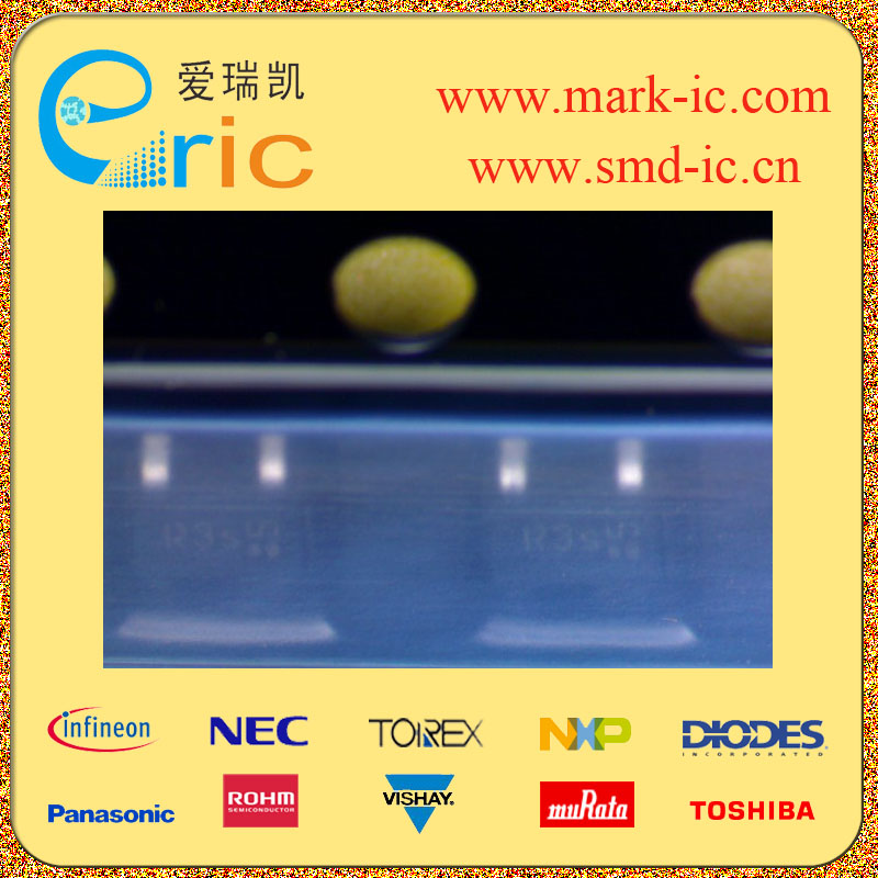
FDS3570 N沟道MOSFET 80V 9A 8-SOIC marking/标记 FDS3570 低漏源导通电阻
| 最大源漏极电压Vds Drain-Source Voltage | 80V |
| 最大栅源极电压Vgs(±) Gate-Source Voltage | 20V |
| 最大漏极电流Id Drain Current | 9A |
| 源漏极导通电阻ΩRds DΩ/Ohmain-SouΩ/Ohmce On-State Ω/Ohmesistance | 22mΩ@ VGS = 6V, ID =8.4A |
| 开启电压Vgs(th) Gate-Source Threshold Voltage | 2~4V |
| 耗散功率Pd Power Dissipation | 2.5W |
| Description & Applications | N-Channel Logic Level Power Trench MOSFET General Description This N-Channel Logic Level MOSFET is produced using Fairchild Semiconductor's advanced Power Trench process that has been especially tailored to minimize on-state resistance and yet maintain superior switching performance. These devices are well suited for low voltage and battery powered applications where low in-line power loss and fast switching are required. Features • Low gate charge • High performance trench technology for extremely low RDS(ON) •High power and current hanling capability |
| 描述与应用 | N沟道逻辑电平功率沟槽MOSFET 概述 这个N-沟道逻辑电平MOSFET采用飞兆半导体先进的功率沟槽进程,已特别是针对减少通态电阻,同时保持出色的开关性能。 这些器件非常适合于低电压和电池供电应用的低线的功率损耗和快速开关是必需的。 特点 •低栅极电荷 •高性能沟道技术极低的RDS(ON) •高功率和电流绫能力 |
| 规格书PDF |