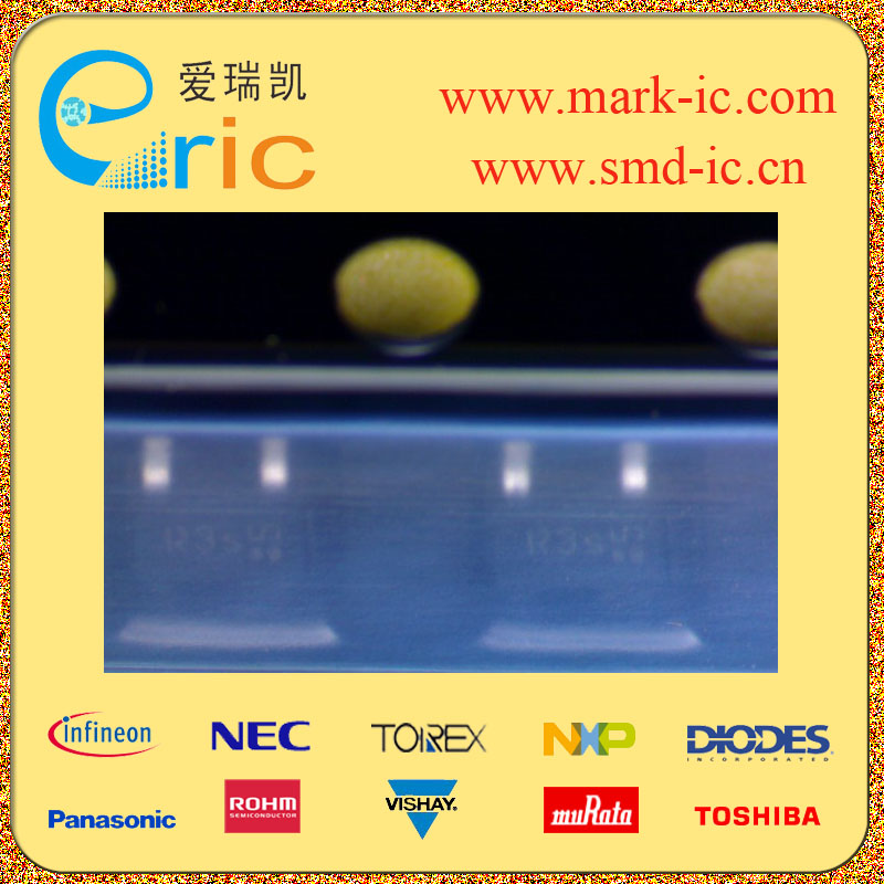
HUF75307D3ST N沟道MOSFET 55V 1.599A TO-252/D-PAK marking/标记 75307D
| 最大源漏极电压Vds Drain-Source Voltage | 55V |
| 最大栅源极电压Vgs(±) Gate-Source Voltage | 20V |
| 最大漏极电流Id Drain Current | 1.599A |
| 源漏极导通电阻ΩRds DΩ/Ohmain-SouΩ/Ohmce On-State Ω/Ohmesistance | 0.090Ω/Ohm @1.5A,10V |
| 开启电压Vgs(th) Gate-Source Threshold Voltage | 2-4V |
| 耗散功率Pd Power Dissipation | 4.5W |
| Description & Applications | 15A, 55V, 0.090 Ohm, N-Channel UltraFET Power MOSFETs These N-Channel power MOSFETs are manufactured using the innovative UltraFET® process. This advanced process technology achieves the lowest possible on-resistance per silicon area, resulting in outstanding performance. This device is capable of withstanding high energy in the avalanche mode and the diode exhibits very low reverse recovery time and stored charge. It was designed for use in applications where power efficiency is important, such as switching regulators, switching converters, motor drivers, relay drivers, owvoltage bus switches, and power management in portable and battery-operated products. • 15A, 55V • Simulation Models Temperature Compensated PSPICE ®and SABER©Models- SPICE and SABER Thermal Impedance Models Available on the WEB at: www.semi.Intersil .com/families/models.htm • Peak Current vs Pulse Width Curve • UIS Rating Curve • Related Literature - TB334, “Guidelines for Soldering Surface Mount Components to PC Boards” |
| 描述与应用 | 15A,55V,0.090欧姆,N沟道UltraFET功率MOSFET 这些N沟道功率MOSFET 使用创新UltraFET®工艺制造。这先进的工艺技术达到尽可能低的导通电阻每硅片面积,造成出色的表现。此设备是能够 承受高能量的雪崩模式和二极管具有非常低的反向恢复时间和存储 收费。它是专为在电源应用中的使用效率是很重要的,如开关稳压器, 开关转换器,电机驱动器,继电器驱动器,低电压总线开关和电源管理在便携式和电池供电产品。 •15A,55V •仿真模型 温度补偿的PSPICE ®和佩剑©模型SPICE和佩剑热阻抗模型 可在网络上: www.semi.Intersil.COM /家庭/ models.htm的 •峰值电流与脉冲宽度曲线 •UIS等级曲线 •相关文献 TB334,“指南焊锡表面装载 组件到PC板 |
| 规格书PDF |