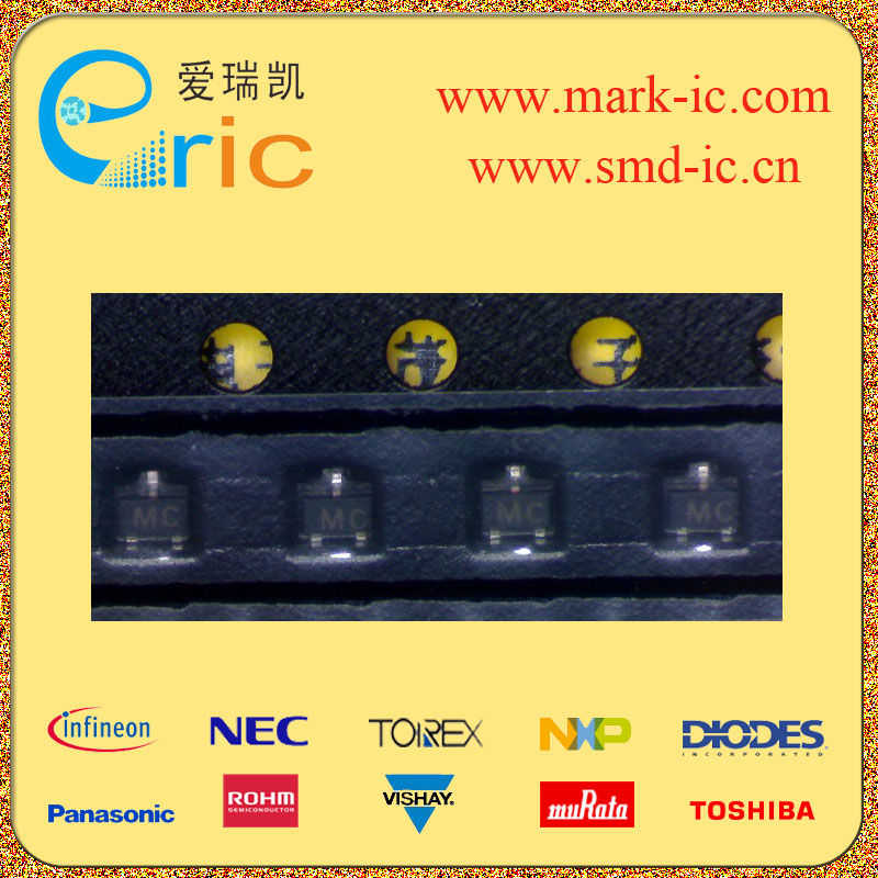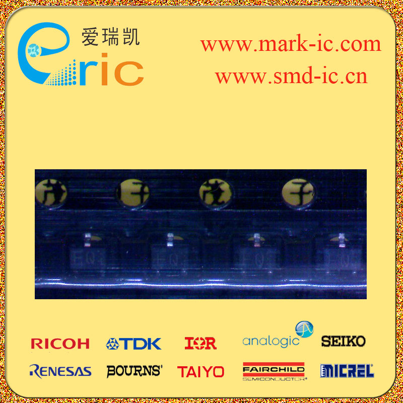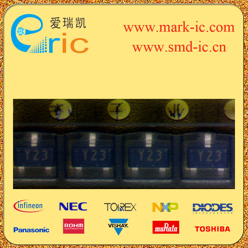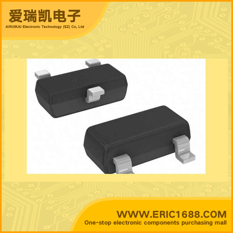
NDS352P P沟道MOS场效应管 -20V 850mA 0.46ohm SOT-23 marking/标记 352
| 最大源漏极电压VdsDrain-Source Voltage | -20V |
| 最大栅源极电压Vgs(±)Gate-Source Voltage | 12V |
| 最大漏极电流IdDrain Current | -850mA/-0.85A |
| 源漏极导通电阻RdsDrain-Source On-State Resistance | 0.46Ω @-800mA,-4.5V |
| 开启电压Vgs(th)Gate-Source Threshold Voltage | -0.8--2.5V |
| 耗散功率PdPower Dissipation | 500mW/0.5W |
| Description & Applications | Proprietary package design using copper lead frame for superior thermal and electrical capabilities. High density cell design for extremely low RDS(ON) .Exceptional on-resistance and maximum DC current capability. Compact industry standard SOT-23 surface mount package. |
| 描述与应用 | 专有包装设计采用铜引线框架的 卓越的热性能和电气性能。 高密度电池设计极低的RDS(ON) 卓越的导通电阻和最大DC电流能力。 紧凑型工业标准SOT-23表面贴装封装 |
| 规格书PDF |