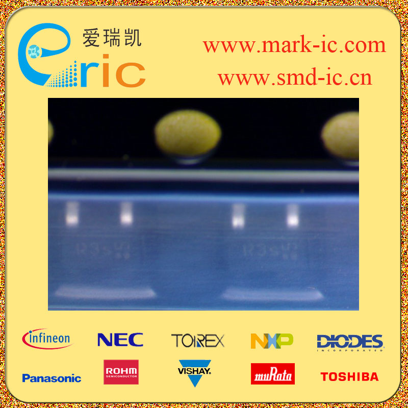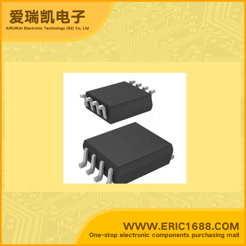
TPC8212 双N沟道场效应管 30V 6A SM8 代码 TPC8212 DC/DC转换器 低漏电流
| 最大源漏极电压VdsDrain-Source Voltage | 30V |
| 最大栅源极电压Vgs(±)Gate-Source Voltage | ±20V |
| 最大漏极电流IdDrain Current | 6A |
| 源漏极导通电阻RdsDrain-Source On-State Resistance | 16mΩ~21mΩ VGS = 10 V , ID = 3 A |
| 开启电压Vgs(th)Gate-Source Threshold Voltage | 1.1V~2.3V VDS = 10 V, ID = 1 mA |
| 耗散功率PdPower Dissipation | 0.75W |
| Description & Applications |
TOSHIBA Field Effect Transistor Silicon N-Channel MOS Type (Ultra-High-Speed U-MOSIII)
High-Efficiency DC/DC Converter Applications
Notebook PC Applications
Portable-Equipment Applications
• Small footprint due to small and thin package
• High-speed switching
• Small gate charge: QSW = 5.5 nC (typ.)
• Low drain-source ON-resistance: RDS (ON) = 16 mΩ (typ.)
• High forward transfer admittance: |Yfs| =14 S (typ.)
• Low leakage current: IDSS = 10 µA (max) (VDS = 30 V)
• Enhancement mode: Vth = 1.1 to 2.3 V (VDS = 10 V, ID = 1 mA)
|
| 描述与应用 |
高效直流/直流转换器的应用程序
笔记本电脑的应用
便携设备应用程序
东芝硅n沟道MOS场效应晶体管(超高速U-MOSIII)类型
由于小和薄包占用空间小
高速开关
小闸极电荷:QSW = 5.5数控(typ)。
低漏源极导通电阻:RDS()= 16 m?(typ)。
高向前转移导纳:| yf | = 14年代(typ)。
低漏电流:ids = 10μA(max)(VDS = 30 V)
|
| 规格书PDF |