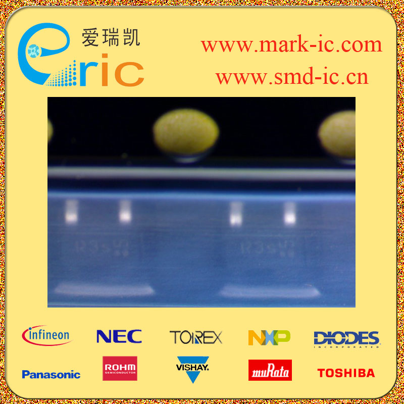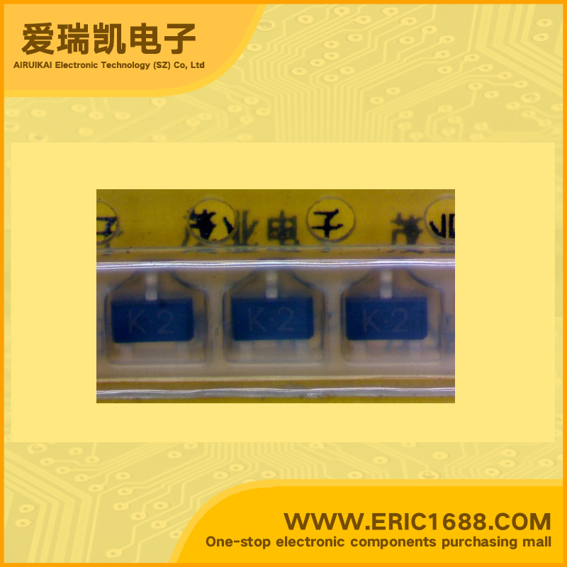
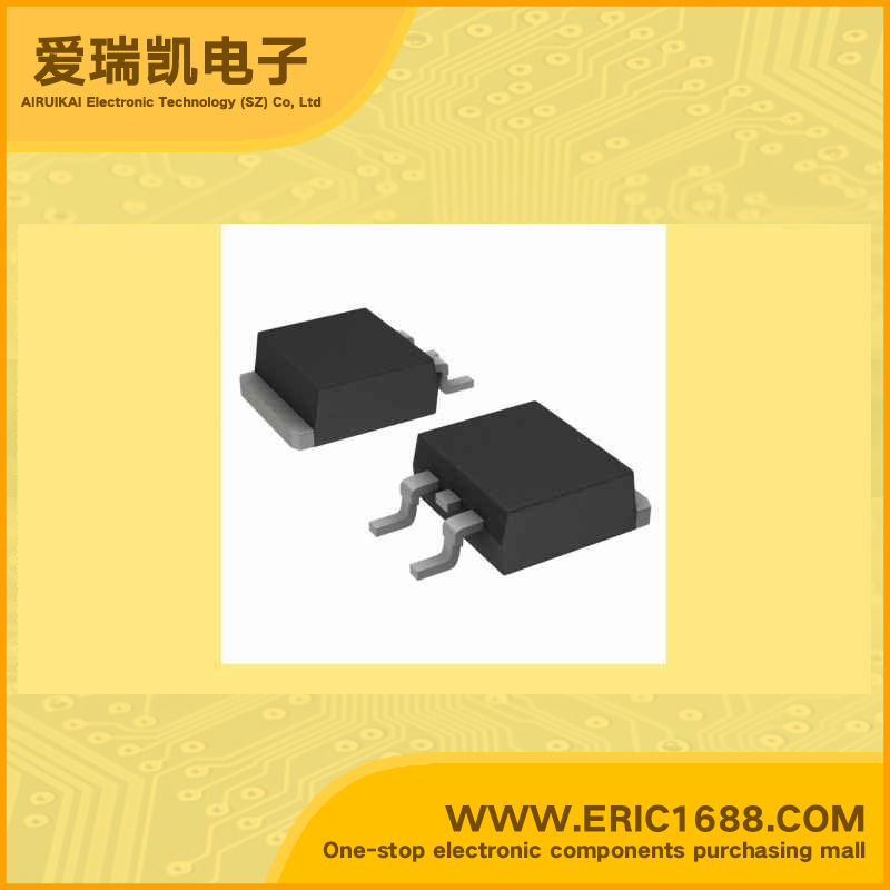
INK0002AC1 N沟道MOSFET 25V 90A TO-252/D-PAK marking/标记 K2 极低的RDS/低栅极电荷/高功率/高电流处理力
| 最大源漏极电压Vds Drain-Source Voltage | 25V |
| 最大栅源极电压Vgs(±) Gate-Source Voltage | 20V |
| 最大漏极电流Id Drain Current | 90A |
| 源漏极导通电阻ΩRds DΩ/Ohmain-SouΩ/Ohmce On-State Ω/Ohmesistance | 0.0032Ω/Ohm 60A,10V |
| 开启电压Vgs(th) Gate-Source Threshold Voltage | 1.2-2V |
| 耗散功率Pd Power Dissipation | 115W |
| Description & Applications | • Ideal for high-frequency dc/dc converters • Qualified according to JEDEC1) for target applications • N-channel, logic level • Excellent gate charge x R DS(on) product (FOM) • Superior thermal resistance • 175 °C operating temperature • Pb-free lead plating; RoHS compliant |
| 描述与应用 | •非常适于高频DC / DC转换器 •符合到JEDEC1) 针对目标应用 •N沟道逻辑电平 •优秀的栅极电荷x R DS(ON) 产品(FOM) •卓越的热电阻 •175°C的工作温度 •无铅引脚电镀,符合RoHS |
| 规格书PDF |