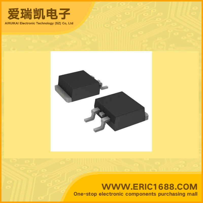
IRFR120N N沟道MOSFET 200V 2.7A TO-252/D-PAK marking/标记 低栅极电荷/极低的RDS/高功率和电流绫能力
| 最大源漏极电压Vds Drain-Source Voltage | 200V |
| 最大栅源极电压Vgs(±) Gate-Source Voltage | |
| 最大漏极电流Id Drain Current | 2.7A |
| 源漏极导通电阻ΩRds DΩ/Ohmain-SouΩ/Ohmce On-State Ω/Ohmesistance | 1.5Ω/Ohm @1350mA,10V |
| 开启电压Vgs(th) Gate-Source Threshold Voltage | 2.0-4.0V |
| 耗散功率Pd Power Dissipation | 2.5W |
| Description & Applications | DESCRIPTION Third generation Power MOSFETs from Vishay provide the designer with the best combination of fast switching, ruggedized device design, low on-resistance and cost-effectiveness. The SOT-223 package is designed for surface-mounting using vapor phase, infrared, or wave soldering techniques. Its unique package design allows for easy automatic pick-and-place as with other SOT or SOIC packages but has the added advantage of improved thermal performace due to an enlarged tab for heatsinking. Power dissipation of greater than 1.25 W is possible in a typical surface mount application. • 2.7A, 200V, RDS(on) = 1.5Ω @VGS = 10 V • Low gate charge ( typical 7.2 nC) • Low Crss ( typical 6.8 pF) • Fast switching • 100% avalanche tested • Improved dv/dt capability |
| 描述与应用 | 说明 Vishay的第三代功率MOSFET提供 设计师与快速切换的最佳组合, 坚固耐用的设备设计,低导通电阻和成本效益。 SOT-223封装是专为表面安装使用气相,红外或波峰焊技术。 其独特的包装设计,可以轻松自动挑选和地方与其他SOT或SOIC封装,但 提高热过往的表现有额外的好处由于散热放大“选项卡。的功耗 大于1.25 W是可能在一个典型的表面贴装应用。 •2.7A,200V,RDS上) =1.5Ω@ VGS= 10 V •低栅极电荷(典型7.2nC) •低Crss(典型6.8 pF) •快速开关 •100%雪崩测试 •改进的dv / dt能力 |
| 规格书PDF |