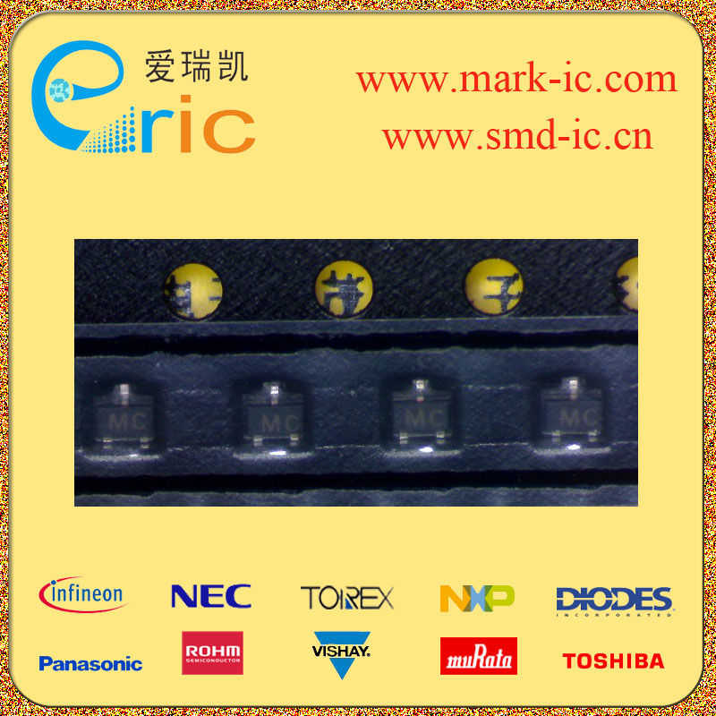
MTD20N03HDLT4 N沟道MOSFET 30V 2A TO-252/D-PAK marking/标记 20N03HL 高速开关/低导通电阻/低电压驱动
| 最大源漏极电压Vds Drain-Source Voltage | 30V |
| 最大栅源极电压Vgs(±) Gate-Source Voltage | 15V |
| 最大漏极电流Id Drain Current | 2A |
| 源漏极导通电阻ΩRds DΩ/Ohmain-SouΩ/Ohmce On-State Ω/Ohmesistance | 0.040Ω/Ohm @10A,4V |
| 开启电压Vgs(th) Gate-Source Threshold Voltage | 1.0-2.1V |
| 耗散功率Pd Power Dissipation | 7.4W |
| Description & Applications | Power MOSFET 20 Amps, 30 Volts, Logic Level N−Channel DPAK This advanced Power MOSFET is designed to withstand high energy in the avalanche and commutation modes. This energy efficient design also offers a drain−to−source diode with a fast recovery time. Designed for low voltage, high speed switching applications in power supplies, converters and PWM motor controls, these devices are particularly well suited for bridge circuits where diode speed and commutating safe operating areas are critical and offer additional safety margin against unexpected voltage transients. • Avalanche Energy Specified • Source−to−Drain Diode Recovery Time Comparable to a Discrete Fast Recovery Diode • Diode is Characterized for Use in Bridge Circuits • IDSS and VDS(on) Specified at Elevated Temperature • Pb−Free Packages are Available |
| 描述与应用 | 功率MOSFET 20安培,30伏特,逻辑电平 N沟道DPAK 这种先进的功率MOSFET的设计可承受高 能源在雪崩和通讯模式。这种高效节能 设计还提供了漏 - 源极二极管具有快速恢复时间。 专为低电压,高速开关应用在电源 用品,转换器和PWM马达控制,这些设备 特别适合于桥电路中二极管的速度和 换向安全工作领域是关键,并提供额外的 对意外的电压瞬变的安全边际。 •雪崩能量 •源漏二极管恢复时间等同于离散 快恢复二极管 •二极管的特点是桥电路中使用 •IDSS和VDS(上) 指定高温 •无铅包可用 |
| 规格书PDF |