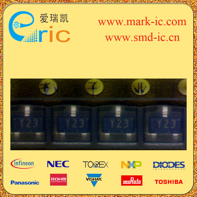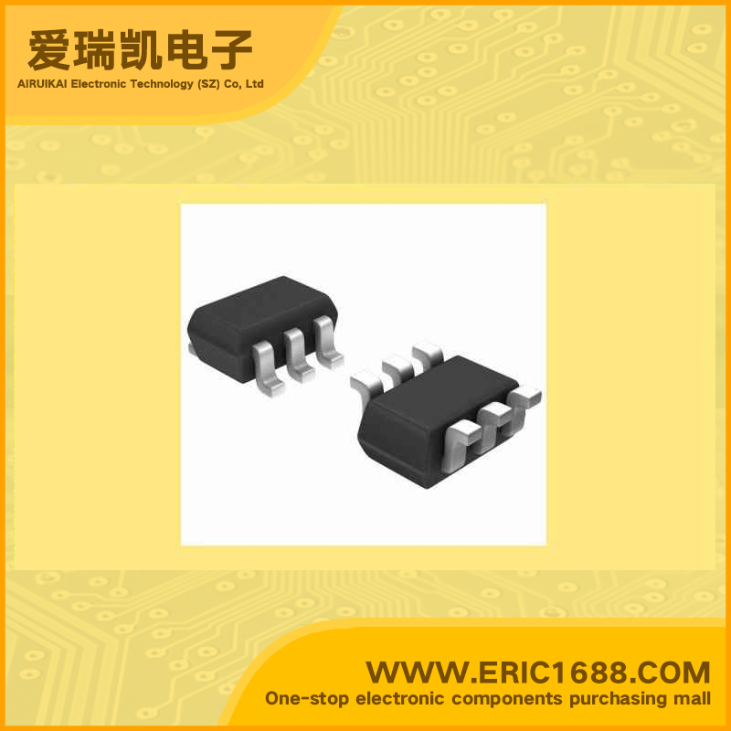
FDG313N N沟道MOSFET 25V 950mA/0.95A SOT-363/SC70-6/TSSOP6/SC-88 marking/标记 13 低导通电阻/超高速开关/4V驱动器
| 最大源漏极电压Vds Drain-Source Voltage | 25V |
| 最大栅源极电压Vgs(±) Gate-Source Voltage | 8V |
| 最大漏极电流Id Drain Current | 950mA/0.95A |
| 源漏极导通电阻ΩRds DΩ/Ohmain-SouΩ/Ohmce On-State Ω/Ohmesistance | 0.45Ω/Ohm @500mA,4.5V |
| 开启电压Vgs(th) Gate-Source Threshold Voltage | |
| 耗散功率Pd Power Dissipation | 750mW/0.75W |
| Description & Applications | Digital FET, N-Channel General Description This N-Channel enhancement mode field effect transistor is produced using Fairchild's proprietary, high cell density, DMOS technology. This very high density process is especially tailored to minimize on-state resistance. This device has been designed especially for low voltage applications as a replacement for bipolar digital transistor and small signal MOSFET. Features • 0.95 A, 25 V. R DS(on)= 0.45 Ω @ V GS = 4.5 V R DS(on)= 0.60 Ω @ V GS = 2.7 V. • Low gate charge (1.64 nC typical) • Very low level gate drive requirements allowing direct operation in 3V circuits (VGS(th) < 1.5V). • Gate-Source Zener for ESD ruggedness (>6kV Human Body Model). • Compact industry standard SC70-6 surface mount package. |
| 描述与应用 | 数字FET,N沟道 概述 这N沟道增强型场效应 晶体管的生产采用飞兆半导体专有的,高 细胞密度,DMOS技术。这非常高密度 特别是针对减少通态过程 阻力。该设备已被特别设计 作为替代低电压应用 双极数字晶体管和小信号MOSFET。 •低栅极电荷(典型值1.64 NC) •非常低的水平栅极驱动要求可直接 操作3V电路(VGS(TH)<1.5V)。 •门源齐纳二极管ESD坚固 (>6kV人体模型)。 •紧凑型工业标准SC70-6表面贴装封装 |
| 规格书PDF |